
|
Optical metrology and inspection for semiconductor devices and manufacturing processes
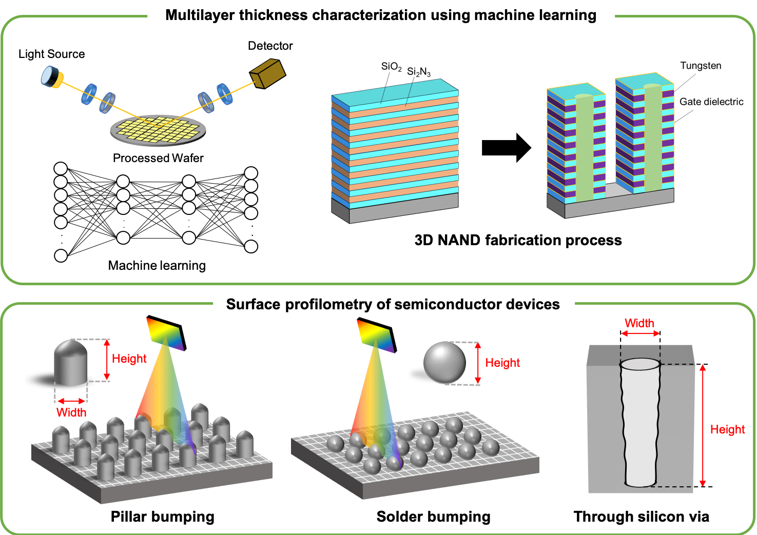
As the demand for data storage continues to soar, from data centers to smart devices, the need for smaller and higher-capacity semiconductor devices is constantly growing. To address this challenge, we are currently working on various problems in the metrology of semiconductor devices during their manufacturing processes with collaboration with several industrial partners. For instance, we've recently developed a non-destructive method for measuring the thickness of individual layers in >200-layer semiconductor multilayer stacks used in 3D-NAND flash memory devices. This technique involves combining optical spectral measurements and machine learning algorithms, enabling us to predict the thickness of each layer with an average root-mean-square error (RMSE) of only 0.16 nm [1,2]. Additionally, we are exploring techniques for rapid, large-scale imaging and height/depth profiling of various 3D semiconductor devices [3,4], building upon our previously demonstrated ultrafast, ultraprecise TOF detection methods [5,6]. As controlling the wafer's temperature is becoming more critical, another area of our research is focused on the development of an ultrafast surface temperature measurement and calibration method for silicon wafers [7].
Related Publications
[1] H. Kwak, S. Ryu, S. Cho, J. Kim, Y. Yang, and J. Kim, "Non-destructive thickness characterisation of 3D multilayer semiconductor devices using optical spectral measurements and machine learning," Light: Advanced Manufacturing 2, 9-19 (2021) 
[2] H. Kwak and J. Kim, "(Invited Review) Semiconductor multilayer nano-metrology with machine learning," Nanomanufacturing and Metrology 6, 15 (2023)
[3] H. Kwak, Y. Na, C. Ahn, J. Bae, and J. Kim, "785-nm frequency comb-based time-of-flight detection for 3D surface profilometry of silicon devices," IEEE Photonics Journal 14, 3150908 (2022)
[4] H. Kwak, J. Bae, Y. Na, S. Ryu, J. Baik, Y. Sohn, and J. Kim, "Frequency comb-based high-speed, large-area surface profilometry," Paper 12618-62, SPIE Optical Metrology 2023
[5] Y. Na, C. Jeon, C. Ahn, M. Hyun, D. Kwon, J. Shin, and J. Kim, "Ultrafast, sub-nanometre-precision and multifunctional time-of-flight detection," Nature Photonics 14, 355-360 (2020)
[6] Y. Na, H. Kwak, C. Ahn, S. Lee, W. Lee, C.-S. Kang, J. Lee, J. Suh, H. Yoo, and J. Kim, "Massively parallel electro-optic sampling of space-encoded optical pulses for ultrafast multi-dimensional imaging," Light: Science & Applications 12, 44 (2023)
[7] J. Bae, M. Hyun, J. Hong, Y. Jeon, S. Son, Y. Seo, S. Ha, and J. Kim, "Optical reflectometry-based high-speed temperature change measurement of silicon wafer surfaces," Paper 12618-82, SPIE Optical Metrology 2023
|
|
|